Semiconductors & Integrated Circuits
Improved High-Power Transistor Amplifier for Wireless Communications
WARF: P08017US
Inventors: Zhenqiang Ma, Guogong Wang, Guoxuan Qin
The Wisconsin Alumni Research Foundation (WARF) is seeking commercial partners interested in developing a high-power, high-gain amplifier capable of amplifying signals at high radio frequencies, making it ideal for wireless communication applications.
Overview
The demand for smaller wireless communication devices that use less power is growing. In particular, radio frequency identification (RFID) systems require small, low-power transmitters to label or “tag” objects. As a result, transistor amplifiers that maximize power handling capability for a given transistor size are desired.
Heterojunction bipolar transistors (HBTs) can handle signals of very high frequencies up to several hundred gigahertz. Modern ultrafast circuits, mostly radio frequency (RF) systems, require high power amplification at high frequencies and typically use HBTs in the final power stages of the signal amplification.
Two common power amplifier configurations for HBTs are the common-base (CB) and common-emitter (CE) configurations. In the CB configuration, the input signal is applied to the emitter of the transistor and the base is at the signal ground. In the CE configuration, the input signal is applied to the base of the transistor and the emitter is at the signal ground.
An improvement in the power handling efficiency of HBTs is necessary within an RF system when increasing the components’ size is not an option. To miniaturize wireless communication applications, an optimal HBT design configuration must be determined.
The Invention
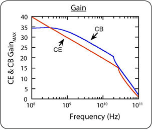
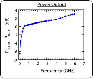
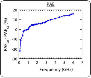
UW-Madison researchers have optimized a high-power amplifier utilizing HBTs with a CB configuration to provide significant improvements in gain and power handling capacity. Although it is widely believed that CB and CE HBT amplifiers should provide identical power, the inventors determined that the power handling capabilities for HBTs are significantly affected by whether they are used in a CB or CE configuration. In voltage source biasing configurations, CE amplifiers provide higher output power than CB configurations. However, if an active current source biasing is used to bias the output of the amplifier, CB amplifiers will outperform CE amplifier configurations using identical parameters.
By taking advantage of the difference between CB and CE configurations, this method provides an increase in power handling for HBT transistor amplifiers without changing the HBT device and most significantly, without increasing the area of the device. In comparison to voltage source biasing configurations, the current source biasing arrangement allows the application of higher voltages since it is not limited by breakdown voltage. The ability to apply higher voltages further expands the opportunities with this new amplifier design, such as an increase in the amplifier gain for improved receiver applications. The amplifier seamlessly integrates with voltage source biasing systems by making the current source bias conversion within the amplifier itself. This improvement in power handling capacity will have a substantial influence on the manufacture and miniaturization of RF amplifiers.
By taking advantage of the difference between CB and CE configurations, this method provides an increase in power handling for HBT transistor amplifiers without changing the HBT device and most significantly, without increasing the area of the device. In comparison to voltage source biasing configurations, the current source biasing arrangement allows the application of higher voltages since it is not limited by breakdown voltage. The ability to apply higher voltages further expands the opportunities with this new amplifier design, such as an increase in the amplifier gain for improved receiver applications. The amplifier seamlessly integrates with voltage source biasing systems by making the current source bias conversion within the amplifier itself. This improvement in power handling capacity will have a substantial influence on the manufacture and miniaturization of RF amplifiers.
Applications
- Wireless power transmissions, particularly automotive collision avoidance, WLAN point-to-point security communications, cell phone applications and other RF devices
- Microwave wireless applications
Key Benefits
- Increases power handling capacity while maintaining the area of the device
- Improves power gain and efficiency more substantially at lower frequencies
- Eliminates need for ballast resistors to improve power gain
- Enables miniaturization of devices requiring high power and high radio frequency bands
- Improves battery life
- Reduces manufacturing costs by increasing yield per wafer
- Reduces power amplifier cost by using more inexpensive semiconductor materials (e.g., allows replacement of III-V with SiGe-based materials)
- Exhibits significantly reduced sensitivity to heating
- Effectively uses the high breakdown voltage of a common-base transistor for improved mismatch ruggedness
Additional Information
For More Information About the Inventors
Tech Fields
For current licensing status, please contact Jeanine Burmania at [javascript protected email address] or 608-960-9846
Figures


